- 您现在的位置:买卖IC网 > Sheet目录238 > NUP4202W1T2G (ON Semiconductor)IC TVS ARRAY HS DATALINE SOT-363
�� �
�
�NUP4202W1�
�ELECTRICAL� CHARACTERISTICS�
�(T� A� =� 25� °� C� unless� otherwise� noted)�
�Symbol� Parameter�
�I� PP�
�Maximum� Reverse� Peak� Pulse� Current�
�V� C�
�Clamping� Voltage� @� I� PP�
�I� F�
�I�
�I� R� V� F�
�V� RWM�
�I� R�
�V� BR�
�Working� Peak� Reverse� Voltage�
�Maximum� Reverse� Leakage� Current� @� V� RWM�
�Breakdown� Voltage� @� I� T�
�V� C� V� BR� V� RWM�
�I� T�
�V�
�I� T�
�Test� Current�
�I� F�
�V� F�
�P� pk�
�C�
�Forward� Current�
�Forward� Voltage� @� I� F�
�Peak� Power� Dissipation�
�Capacitance� @� V� R� =� 0� and� f� =� 1.0� MHz�
�I� PP�
�Uni� ?� Directional� TVS�
�*See� Application� Note� AND8308/D� for� detailed� explanations� of�
�datasheet� parameters.�
�ELECTRICAL� CHARACTERISTICS� (T� J� =25� °� C� unless� otherwise� specified)�
�Parameter�
�Symbol�
�Conditions�
�Min�
�Typ�
�Max�
�Unit�
�Reverse� Working� Voltage�
�Breakdown� Voltage�
�Reverse� Leakage� Current�
�V� RWM�
�V� BR�
�I� R�
�(Note� 2)�
�I� T� =� 1� mA,� (Note� 3)�
�V� RWM� =� 5� V�
�6.0�
�5.0�
�5.0�
�V�
�V�
�m� A�
�Clamping� Voltage�
�Clamping� Voltage�
�Maximum� Peak� Pulse� Current�
�Junction� Capacitance�
�Junction� Capacitance�
�Clamping� Voltage�
�Clamping� Voltage�
�V� C�
�V� C�
�I� PP�
�C� J�
�C� J�
�V� C�
�V� C�
�I� PP� =� 5� A� (Note� 4)�
�I� PP� =� 8� A� (Note� 4)�
�8x20� m� s� Waveform� (Note� 4)�
�V� R� = 0 V, f = 1 MHz between I/O Pins and GND�
�V� R� =� 0� V,� f� =� 1� MHz� between� I/O� Pins�
�@� I� PP� =� 1� A� (Notes� 5� and� 6)�
�Per� IEC� 61000� ?� 4� ?� 2� (Note� 7)�
�8.5�
�8.9�
�3.0�
�1.5�
�14.5�
�Figure� 1� and� 2�
�12.5�
�20�
�28�
�5.0�
�3.0�
�V�
�V�
�A�
�pF�
�pF�
�V�
�V�
�2.� TVS� devices� are� normally� selected� according� to� the� working� peak� reverse� voltage� (V� RWM� ),� which� should� be� equal� or� greater� than� the� DC�
�or� continuous� peak� operating� voltage� level.�
�3.� V� BR� is� measured� at� pulse� test� current� I� T� .�
�4.� Nonrepetitive� current� pulse� per� Figure� 5� (Pin� 5� to� Pin� 2).�
�5.� Nonrepetitive� current� pulse� per� Figure� 5� (Any� I/O� Pins).�
�6.� Surge� current� waveform� per� Figure� 5.�
�7.� For� test� procedure� see� Figures� 3� and� 4� and� Application� Note� AND8307/D.�
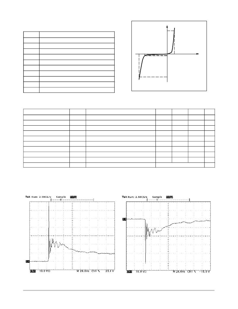
�Figure� 1.� ESD� Clamping� Voltage� Screenshot�
�Positive� 8� kV� Contact� per� IEC61000� ?� 4� ?� 2�
�Figure� 2.� ESD� Clamping� Voltage� Screenshot�
�Negative� 8� kV� Contact� per� IEC61000� ?� 4� ?� 2�
�http://onsemi.com�
�2�
�发布紧急采购,3分钟左右您将得到回复。
相关PDF资料
NUP4212UPMUTAG
TVS QUAD ARRAY LOW CAP 6-UDFN
NUP4302MR6T1
IC DIODE ARRAY SCHOTTKY TSOP6
NUP4304MR6T1
IC DIODE ARRAY LO CAP ESD SC74-6
NUP45V6P5T5G
TVS QUAD ARRAY LOW CAP SOT-953
NUP46V8P5T5G
TVS QUAD ARRAY LOW CAP SOT-953
NUP5120X6T2G
IC TVS ARRAY 5LINE SOT-563
NUP5150MUTBG
IC TVS ARRAY 5LINE ESD 6-UDFN
NUP6012PMUTAG
TVS ESD 6CH LOW CAP 6-UDFN
相关代理商/技术参数
NUP4212UPMU
制造商:ONSEMI 制造商全称:ON Semiconductor 功能描述:Quad Transient Voltage Suppressor Array
NUP4212UPMUTAG
功能描述:TVS二极管阵列 ULTR LO CAPACITANCE ESD PRTCT ARRAY RoHS:否 制造商:Littelfuse 极性: 通道:4 Channels 击穿电压: 钳位电压:11.5 V 工作电压:2.5 V 峰值浪涌电流:20 A 安装风格:SMD/SMT 端接类型:SMD/SMT 系列: 最小工作温度:- 40 C 最大工作温度:+ 85 C
NUP4301
制造商:ONSEMI 制造商全称:ON Semiconductor 功能描述:Low cap. diode array for 2 Line High Speed USB protection devic
NUP4301MR6T1
功能描述:整流器 Low Cap. for ESD RoHS:否 制造商:Vishay Semiconductors 产品:Standard Recovery Rectifiers 配置: 反向电压:100 V 正向电压下降: 恢复时间:1.2 us 正向连续电流:2 A 最大浪涌电流:35 A 反向电流 IR:5 uA 安装风格:SMD/SMT 封装 / 箱体:DO-221AC 封装:Reel
NUP4301MR6T1/D
制造商:ONSEMI 制造商全称:ON Semiconductor 功能描述:Low Capacitance Diode Array for ESD Protection in Four Data Lines
NUP4301MR6T1_05
制造商:ONSEMI 制造商全称:ON Semiconductor 功能描述:Low Capacitance Diode Array for ESD Protection in Four Data Lines
NUP4301MR6T1G
功能描述:整流器 Low Cap. for ESD Protection in 4 Line RoHS:否 制造商:Vishay Semiconductors 产品:Standard Recovery Rectifiers 配置: 反向电压:100 V 正向电压下降: 恢复时间:1.2 us 正向连续电流:2 A 最大浪涌电流:35 A 反向电流 IR:5 uA 安装风格:SMD/SMT 封装 / 箱体:DO-221AC 封装:Reel
NUP4301MR6T1G
制造商:ON Semiconductor 功能描述:TVS DIODE ARRAY 70V TSOP 制造商:ON Semiconductor 功能描述:TVS DIODE ARRAY, 70V, TSOP